America Lehighton Electronics(LEI) product: the sheet resistance is measured by eddy current principle without contact the block.
Application: all compound semiconductors, such as SiC, GaAs (epitaxial layer, semi-insulating substrate, doped substrate, annealing ion implantation), silicon wafer (body silicon, epitaxial, ion implantation, POCl3 doped on high-resistance substrate), metal film, etc.
| LEI 1510M40 | |||
| Range | sheet resistance Ω/sq | repeatability% | bulk resistivity Ω-cm |
| HI | 3000 | 2.50 | 200 |
| 400 | 0.40 | 25 | |
| 15 | 0.20 | 1 | |
| LO | 15 | 1.50 | 1 |
| 2 | 0.50 | 0.1 | |
| 0.2 | 0.50 | 0.01 | |
| XL | 1.5 | 0.70 | 0.1 |
| 0.2 | 0.55 | 0.01 | |
| 0.035 | 0.55 | 0.005 | |
| remarks:pure manual control, without computer;sample size15——200mm | |||
.jpg)
| LEI88 | |
| Range | sheet resistance Ω/sq |
| HI | 16 - 3,200 ohms/sq |
| LO | 0.16 - 16.0 ohms/sq |
| XL | 0.032 - 1.6 ohms/sq |
| remarks: include a laptop, the largest sample 150mm | |

| LEI 1510E | |||
| Range | sheet resistance Ω/sq | repeatability% | bulk resistivity Ω-cm |
| HI | 3000 | 2.50 | 200 |
| 600 | 0.40 | 25 | |
| 15 | 0.20 | 1 | |
| LO | 15 | 1.50 | 1 |
| 1.6 | 0.50 | 0.1 | |
| 0.16 | 0.50 | 0.01 | |
| XL | 1.6 | 0.70 | 0.1 |
| 0.16 | 0.55 | 0.01 | |
| 0.035 | 0.55 | 0.005 | |
| remarks: Mapping function,2D/3D graphic output, data output;optional light shield2-8inches | |||

| LEI 1510ERP | |||
| Range | sheet resistanceΩ/sq | repeatability% | bulk resistivityΩ-cm |
| HI | 3000 | 2.50 | 200 |
| 600 | 0.40 | 25 | |
| 15 | 0.20 | 1 | |
| LO | 15 | 1.50 | 1 |
| 1.6 | 0.50 | 0.1 | |
| 0.16 | 0.50 | 0.01 | |
| XL | 1.6 | 0.70 | 0.1 |
| 0.16 | 0.55 | 0.01 | |
| 0.035 | 0.55 | 0.005 | |
| remarks: Mapping function,2D/3D graphic output, data output;optional light shield2-8inches | |||
.jpg)
| LEI 1510ERS | ||||
| Range | sheet resistanceΩ/sq | repeatability% | bulk resistivityΩ-cm | |
| HI | 3000 | 2.50 | 200 | |
| 600 | 0.40 | 25 | ||
| 15 | 0.20 | 1 | ||
| LO | 15 | 1.50 | 1 | |
| 1.6 | 0.50 | 0.1 | ||
| 0.16 | 0.50 | 0.01 | ||
| XL | 1.6 | 0.70 | 0.1 | |
| 0.16 | 0.55 | 0.01 | ||
| 0.035 | 0.55 | 0.005 | ||
| remarks:1.Mapping function,2D/3D graphic output, data output;optional light shield, 2-8inches | ||||
| 2.with another type 300mm 12inches LEI RS300 | ||||
.jpg)
| LEI 1800LS Special for flat panel display and solar cells with mapping(Manual) | |
| Range | sheet resistance Ω/sq |
| HI | 15 - 3,200 |
| LO | 0.16 - 16.0 |
| XL | 0.032 - 1.6 |
| remarks: include a laptop; precision +/-5%;sample75*75—600*600, thickness reached 12mm | |

| LEI 1800AG Gantry Special for flat panel display and solar cells with mapping(Auto) | |
| Rate | 10-point Per Minute |
| Sample | Max 1000mm×1100mm |
| Mapping | Yes |

1.2 Contactless Carrier Mobility/Carrier Density/Sheet Resistance Measurement and Mapping Systems
America Lehighton Electronics(LEI)
| Parameters and systems | 1610E100M | 1610E00AM | 1610E100AM-RP |
| magnet | electromagnet(1.0T) | ||
| mobility(cm2/v.sec) | 100-20000 | ||
| sheet resistance(ohm/sq) | 100-3000 | ||
| charge carrier surface density(cm-2) | 1E11-1E14 | ||
| dynamic repeatability(mobility/surface density) | 4.0% | 3.0% | 3.0% |
| dynamic repeatability(sheet resistance) | 3.0% | 2.0% | 2.0% |
|
static and dynamic repeatability(mobility/ surface density/sheet resistance) |
2.0% | 1.0% | 1.0% |
| sample size | 2"-8"inches | ||
| probe coil diameter | 21mm(optional 14mm) | ||
| Mapping | Max 9 points | Max 55 points | Max 55 points |
| Wafer Loading | manual | manual | auto |
| Wafer Positioning | manual | auto | auto |
LEI-1600系列非接触迁移率测量系统是半导体生产工艺控制、产品质量监测和提高产品率的检测设备, 常应用于无损测量化合物半导体材料的迁移率、载流子浓度、方块电阻。测量样品包括GaAs (pHEMT, HEMT, HBT), GaN(HEMT, LED), SiC, SiGe, InP, Si等的外延结构。
![]() 无需破坏、切割昂贵的样品, 实现大样品mapping
无需破坏、切割昂贵的样品, 实现大样品mapping
![]() 无需腐蚀, 不改变样品的特性
无需腐蚀, 不改变样品的特性
![]() 不再需要制作恼人的电极
不再需要制作恼人的电极
![]() 可同时分析多层载流子
可同时分析多层载流子
.jpg)
.jpg)
.jpg)


| Model | Size | Mapping | The connected instrument |
| 802B-150-6" | 150mm | no |
1 MHz: Boonton 7200, 1 MHz capacitance/conductance, +/- 100 Volts Variable Frequency: Agilent E4980A capacitance/conductance (20 Hz to 2 MHz), +/- 40 Volts Agilent 4285A capacitance/conductance (75 kHz to 30 MHz), +/- 40 Volts Agilent B1500A Semiconductor Device Analyzer (1 kHz to 5 MHz), +/- 25 / 100 Volts Keithley 4200 capacitance/conductance (1 Hz to 10 MHz), +/- 200 Volts Agilent 4294A Precision Impedance Analyzer (40 Hz to 110 MHz), +/- 40 Volts Quasi-static: Agilent 4140B, +/- 100 Volts (Refurbished Only) Agilent B1500A, +/- 25 / 100 Volts Keithley 4200, +/- 200 Volts Current Meters: Keithley 4200, +/- 200 Volts Keithley 2600 Series, +/- 40 or 200 Volts Keithley 2400 Series, +/- 200 / 1100 Volts Keithley 237, +/- 1100 Volts Agilent 4140B, +/- 100 Volts (Refurbished Only) Agilent B1500A Semiconductor Device Analyzer, +/- 100 Volts |
| 802B-200-8" | 200mm | no | |
| 862B-12" | 300mm | yes | |
| 864B-14" | 355mm | yes | |
|
Customizable size、Customizable mercury contact area SiC、GaN measurement Can upgrade computer positioning control(802C/862C) |
|||
1.4 Four-Point Probe Mapping Systems(4PP)
AIT CO., LTD.


| Model | Measurements size | Measurement range | Measurement precision | Probe | Computer control/mapping |
| SR1000N | 8inches/140*140mm | 1mohm/sq——2Mohm/sq | 0.5% VLSI |
England Jandel original probe gap:25-50mils(gap5mils) pressure:10g/pin-250g/pin needle radius:12.5-500micron |
LCD panel display |
| SR2000N | 8inches | Yes | |||
| SR2000N-PV | 156*156mm | ||||
| SR3000 | user customization | ||||
| SR5000 | 12inches/210*210mm |
1.5 Plasma spectrum analyzer
Germany Mikropack GmbH
| Parameters | |
| wavelength coverage: | 200—1100nm |
| wavelength resolution: | 1nm half width |
| application: | vapor film deposition |
| plasma etching | |
| surface cleaning | |
| magnetron sputtering | |
| optical coating | |
| end-pointing | |
.jpg)
1.6 Multifunction HAWK-1000 Peel Force Tester
CE TEK CO., LTD.
| index characteristics | |
| control software: | windows graphic software, function include control, calibration, analysis, SPC, etc. |
| X/Y stage: | customizable:50--450mm |
| X/Y/Z/θ control: | about speed joystick |
| test control: | left joystick button to trigger |
| operational height rollback: | right joystick button to trigger |
| test module: | Wire tension module |
| Die shear module | |
| Stud tension module | |
| Fierce collision module | |
| Pliers tension module | |
| optical image system: | YES |
| standards and certification: | JEDEC、MILS、EIA、ISO9001、ISO14001, etc. |

1.7 Hand-held Pencil HAWK-1000 Peel Force Tester
CE TEK CO., LTD.
main characteristics
1. thread tension、ball shear force、die shear force、SMT shear force measurement
2. tension accuracy max up±0.2%
3. options:100g、500g、1Kg、5Kg
4. LCD display, output to PC with USB
5. can upgrade to manual tension、shear force tester

1.8 PIND Particle Impact Noise Detection
America SPECTRAL DYNAMICS
Particle Impact Noise Detection (PIND) which is by colliding the electronic components, such as transistor integrated circuit hybrid diode relay and switching equipment, loose the fine particles in the inner cavity, and generates a sound signal. So, the PIND judge the integrity of electronic components by means of the sound signal
颗粒碰撞噪声侦测往往用于电子元件的完整制造,因为它被认为是检测成品经济又有效的最好方法。PIND测试已被写入最广泛应用的军用标准883-方法2020, 军用标准750-方法2052, 军用标准202F-方法217, 军用标准39016-中,同时也被列入微电路和半导体S级别的要求。

| Main Technical Parameters | |
| Vibration impact range: | 100-2500G;(resolution 10G) |
| Vibration frequency range: | Sine 25-250Hz; (resolution 1Hz); optional random waveform |
| Vibration amplitude range: | 0.1-25.50G; (resolution 0.1G) |
| Noise sensor sensitivity: | -77.5±3dB re 1V per Microbar at 155 kHz (ANSI 2.1-1988) |
| Single sensor sensitive area: | 0.75” radius circular region |
| Max number of noise sensors on the table: | 5 |
| Table size: | diameter50mm, 100mm or 150mm, or rectangular table 150x50mm |
| Max quality device: | 1200Grams |
1.9 Film Stress & Wafer Bow Measurement System
America Frontier Semiconductor (FSM)
| FSM integrate the world's leading non-destructive laser scanning technology, can scan 40 data points per millimeter and produce 2D 3D color pictures quickly. | ||
| room temperature system | FSM 128 | max sample diameter 200mm |
| FSM 128L | max sample diameter 300mm | |
| FSM 128G | max sample 550×650mm | |
| variable temperature system | FSM 500TC | resistance heating table:temperature controlled, top to 500℃ |
| FSM 900TC-vac | RTP type chamber: temperature controlled, top to 900℃(option 1100℃); vacuum 1E-6 Torr | |

1.10 Ellipsometer, Spectral ellipsometer
America J. A. Woollam Co.
model: M-2000
M-2000 have a wide variety of configurations, such as multiple wavelength range and angular variation, the rotating compensation patented technology ensures the measurement accuracy, the high speed CCD enable that the full spectrum scanning can be completed in a matter of seconds.


| M-2000 main technical parameters | |
| detector:CCD | data acquisition time:3s (fast mode), 10s (standard mode), 30s (long time mode) |
| signal accuracy*:Ψ = 45°± 0.075° Tan(Ψ)=1±0.0013 Δ = 0° ± 0.05° Cos(Δ)=1± 0.0000015 * incident beam direct measurement without sample, 95% measured wavelengths met the above criteria |
thickness repeatability *:Std.Dev = 0.02 Å(standard deviation) * 30times retest sample SiO2(25nm)/Si-sub, 70°incident angle |
| collimating beam and light spot: elliptic type 2-5mm min light spot 25X60um (the quotation is subject to different configurations) |
automatic sample movement table:XY direction 300mm X 300mm |
| max sample size:Φ300mm | max sample thickness:20mm |
model:Alpha-SE
This is a cost-effective manual variable angle spectrum ellipsometer, the rotating compensation patented technology ensures the measurement accuracy, the high speed CCD enable that the full spectrum scanning can be completed in a matter of seconds.


| Alpha-SE main technical parameters | |
| Spectral range::380nm to 900nm (180 wavelength) | detector:CCD |
| Incident angle: 65°、70°、75°、 90°, convenient conversion | Computer connection mode: USB |
| The height of sample table is adjusted automatically | Data acquisition time: 3s (fast mode), 10s (standard mode), 30s (long time mode) |
| Signal accuracy *:Ψ = 45°± 0.1 Δ = 0° ± 0.2 * incident beam direct measurement without sample, 98% measured wavelengths met the above criteria |
thickness repeatability *: Std.Dev = 0.15 Å (standard deviation) * 30times retest sample SiO2(25nm)/Si-sub, 70°incident angle |
model:VASE
VASE-Variable Angle Spectroscopic Ellipsometer is a precise and universal ellipsometer, is applicable to study and analyze all types of materials: semiconductor、dielectric、polymer、metal、multilayer, etc.


| VASE measurement parameters | wavelength coverage |
| the reflective and perspective measurement of Ellipsometry | spectral region:240-1100nm |
| the measurement of transmissivity(T) and reflectivity(R) | Uv extension 193-1100nm |
| the anisotropic material、birefringence material、phase hysteresis material measurement of Ellipsometry | first grade near-infrared extension 1100-1700nm |
| the measurement of cross polarization R/T/T测量 | second grade near-infrared extension 1100-2500nm |
| the measurement of depolarization and scattering | third grade near-infrared extension 1100-3200nm |
| the measurement of Mueller matrix | variable Angle range: 20º-90º angular accuracy: 0.01º |
model:IR-VASE
IR-VASE is the first and only spectral ellipsometer with spectral coverage ranging from 1.7 to 30 microns (333 to 5900 wavenumbers), IR-VASE is suitable for thin film or bulk materials, including dielectric, semiconductor, polymer and metal.


| IR-VASE main technical parameters | |
| spectral range:1.7 - 33µm | variable angle range 26º-90º |
|
signal accuracy *:Tan(Ψ)=1±0.004
Cos(Δ)=1±0.0001 * incident beam direct measurement without sample, wave number 300 to 5000 cm-1 |
signal repeatability *:Std.Dev = ±0.0004(Tan(Ψ)的standard deviation Std.Dev = ±0.0000003 (Cos(Δ) standard deviation) * wave number 2000 cm-1 |
model:VUV-VASE
VUV-VASE-Variable Angle spectral ellipsometer, it can measures the range from deep ultraviolet (VUV) to near infrared (NIR), including dielectric, semiconductor, polymer, metal and liquid.


| VUV-VASE main technical parameters | |
| sample size:200mm | spectral range:140-1700nm |
| variable angle range:10º-90º (wavelength<300nm), 25-90º (wavelength >300nm) | |
model:T-Solar
T-Solar is a spectral ellipsometer that tailored for the photovoltaic industry, combined with the best photoelectric measurement technology, specially designed for texture samples.


| T-Sloar main technical parameters | |
| wavelength coverage: 245-1000nm, 470个波长点 | incident angle:45º-90º |
| sample stage variable Angle (Tilt): 0º-60º | |
1.11 NanoMap Series 3D Surface Profilometer
America AEP Technology, Inc.
| NanoMap-D Two – mode, three - dimensional surface profilometer | ||
| The world's first and only profiler which is capable of both probe scanning and white light interference scanning. | ||
| 3D contact profiler | step repetitive rate | 5A |
| fine mode Z height range | 5μm | |
| coarse mode Z height range | 500μm(可选1.5mm) | |
| tip Scan mode(XY) | max50μm | |
| stage Scan mode(XY) | max150mm(optional 200mm, etc.) | |
| probe pressure | 0.03-100mg | |
| sample table | 150*150mm(optional 200*200mm, etc.) | |
| 3D non-contact optical profiler | step repetitive rate | 1A |
| CCD resolution | 1024*1024/1536*1536/1920*1920 | |
| objective lens | 2.5x/5x/10x/20x/50x/100x | |
| sample reflectance | 0.4-100% | |
| max sample thickness | 50mm(optional 100mm) | |
| sample table rotation | 360 degree | |
| sample table incline | 4 degree | |
| stress analysis | ||

.jpg)
| NanoMap-500LS Probe 3d profiler | |||
| model | NanoMap-500LS | NanoMap-LS | NanoMap-ES |
| basic technical parameters | there are two modes of probe scanning (Tip) and sample Stage scanning (Stage), it can be used to measure the large area of the long distance or to obtain the optimized two-dimensional/three-dimensional observation map of small area. Short-range probe scanning uses a precise piezoelectric ceramic to drive the scanning mode, the 3d scanning range from 10μm X 10μm to 500μm X 500μm, subnanometer vertical resolution (min 0.1 nm); Long-range sample table scanning using advanced optical reference platform, scanning range can be reach to 150 mm. | ||
| step repetitive rate | 5A | ||
| fine mode Z height range | 5μm | ||
| coarse mode Z height range | 500μm(optional 1.5mm) | ||
| tip scan mode(XY) | max 500μm | NO | max 500μm |
| stage scan mode(XY) | max 150mm(optional 200mm, etc.) | max 300mm | |
| probe pressure | 0.03-100mg | ||
| sample table | 150*150mm(optional 200*200mm, etc.) | 300*300mm | |
| max sample thickness | 50mm(optional 100mm) | ||
| sample table rotation | 360 degree | ||
| sample table incline | 4 degree | ||
| stress analysis | Yes | ||

.png)
.png)
| NanoMap-1000WLI white light interferometer | |
| White light interference brings high resolution, 4 megapixel images, and wide range scans, with using the PSI(phase shift interferometry)technology, without touching and damage the surface of the sample, and no requirements of the surface hardness, and can even test the viscoelastic sample. | |
| light source | long-period LED with two-echelon bandpass filtering grating technology |
| optional objective lens multiple | 10x (standard), 2.5x, 5x, 20x, 50x, 100x |
| vertical resolution | 0.1 Å |
| digital zoom | 1x, 2x |
| RMS repeatability | 1 Å |
| vertical scanning speed | 3.75 to 26um/sec(software controllable) |
| max vertical measurement range | 20mm |
| step height repetitive rate | 0.1% or 1 Å (1 sigma) |
| step repetition rate | 1 Å |
| CCD resolution | 1024 x 1024(standard), 1536 x 1536 , 1920 x 1920 |
| objective lens | 2.5x/5x/10x/20x/50x/100x |
| Z scan range | 20mm |
| sample reflectance | 1% to 100% |
| sample table rotation | 360 degree |
| sample table incline | Max 4 degree |
| standard sample | 8μm steps prototype(options) |
| sample table | 150*150mm(optional 300*300mm) |
| max sample thickness | 50mm(optional 100mm) |
| sample table rotation | 360 degree |
| sample table incline | 4 degree |

.png)
| major function |
|
| Precision P-1000 is widely used in the fields of semiconductor, superconductor and magnetic materials | ||
| model | Precision P-1000 | |
| sample size | 8 inches(options 12 inches) | |
| X-ray spectrometer | WDX and EDX | |
| X-ray sources | 30KV - 20mA | |
| application |
|
|
.jpg)
1.13 Surface Contact Angle Gauge
Italy SCI Automation CO. LTD
| CAM 2 is a desktop manual surface contact angle meter, is suitable for measuring the contact angle of semiconductor substrate and lead frame, verify the surface energy before and after the plasma cleaning process an used in the ultra-clean room. | |||
| model | CAM 2 | ||
| machine size | 1140 x 560 x 465(height)mm | ||
| sample size | less than 200*200*5mm | ||
| compressed air | dry, pressure 3-6 bar | ||
| workbench | 280*280mm(options:can heat up to 150℃) | ||
| XYZ | X | 250mm | |
| Y | 250mm | ||
| Z | 20mm | ||
| measure Mode | datum line | equipment with | vacuum interface, 17 inches display/computer control |
| arch datum line | stainless steel base plate fixation needle | ||
| double arch | integrated sub-micro upgraded drip needles | ||
| contour line | highlight LED backlight, HD camera | ||


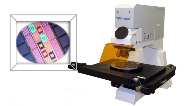
1.14 TFProbe MSP300
Angstrom Sun Technologies Inc
| Model | MSP300R-M150 |
| Detector | CCD Array with 2048 pixels |
| Light Source | Halogen Lamp |
| Automatic Stage | Black Anodized Aluminum Alloy with 6”x6” net travel distance and 0.1µm resolution, program controlled |
| Long Working Distance Objectives | 10x, 50x |
| Communication | USB |
| Digital Imaging | 1280x1000 Pixels |
| Measurement Type | Reflection spectra, Film thickness/refractive index and feature dimensions |
| Computer | Intel Duo Core Processor with 200GB Hard drive and DVD+RW Burner plus 19” LCD Monitor or Laptop equivalent |
| Software | TFProbe 2.4 |
| Dimension | 20’x20’x24’ (Table top setup) |
| Weight | ~120 lbs total |
| Power | 110– 240 VAC /50-60Hz, 3A |
| Warranty | One year labor and parts |